


- GL823A-06

- 参考价格:
- 发布者:korechipic
- 查看更多 GL823A-06 供应商 获取更低报价

|
查看此店铺所有供求信息 联系人:颜先生 电话:0755-21001680 手机:13925219291 地址:深圳市龙华新区民治梅陇路南源商业大厦1105室 服务: 价格: 综合: 营业时间:全年营业 QQ/微信/Skype:  |
详细信息
品牌:GENESYS/创惟科技
封装:QFN-24A
批号:23+
数量*:9000
描述:GL823A-06 电子元器件 GENESYS/创惟科技 封装QFN-24A USB 2.0 SD/MMC读卡器单芯片
GENERAL DESCRIPTION
The GL823 is a USB 2.0 SD/MMC Flash Card Reader single chip. It supports USB 2.0 high-speed transmission
to Secure DigitalTM (SD), SDHC, SDXC, miniSD, microSD (T-Flash), MultiMediaCardTM (MMC), RS-MMC,
MMCmicro, MMCmobile on one chip. As a single chip solution for USB 2.0 flash card reader, the GL823
complies with Universal Serial Bus specification rev. 2.0, USB Storage Class specification ver.1.0, and
SD/MMC card interface specification.
The GL823 integrates a high speed 8051 microprocessor and a high efficiency hardware engine for the best data
transfer performance between USB and flash card interfaces. Its’ pin assignment design fits to card sockets to
provide easier PCB layout. Inside the chip, it integrates 5V to 3.3V and 3.3V to 1.8V regulators and power
MOSFETs and it enables the function of on-chip clock source (OCCS) which means no external 12MHz XTAL
is needed and that effectively reduces the total BOM cost.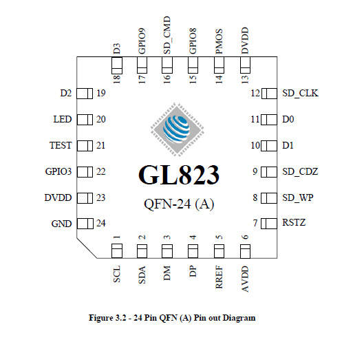
法律声明:本站只提供信息交流平台,各交易者自己审辨真假,如有损失,本站概不负责。
警方提示:网上买、卖商品要谨慎小心,以免上当受骗。
警方提示:网上买、卖商品要谨慎小心,以免上当受骗。
所有评论
商品评论()
最新评论