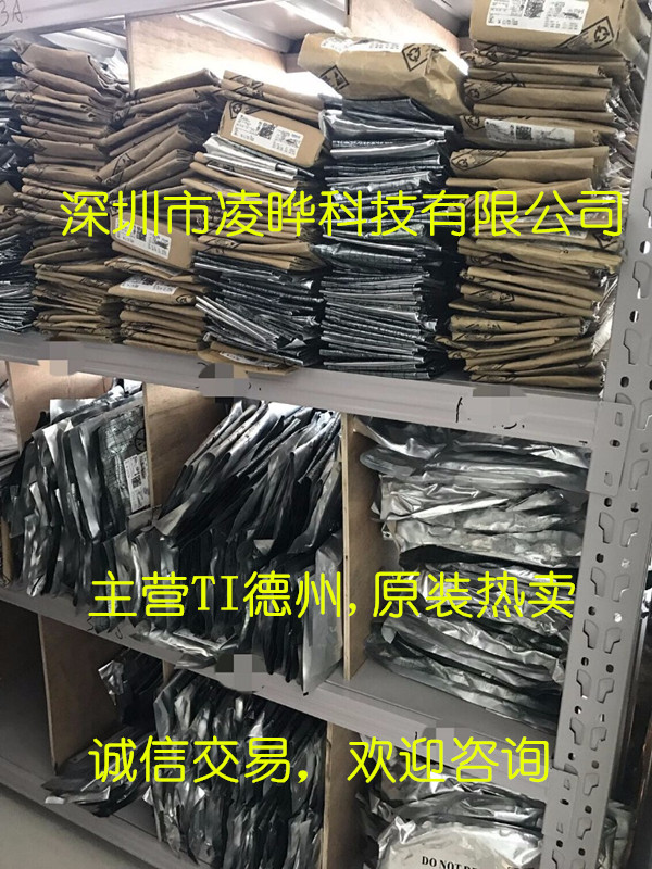
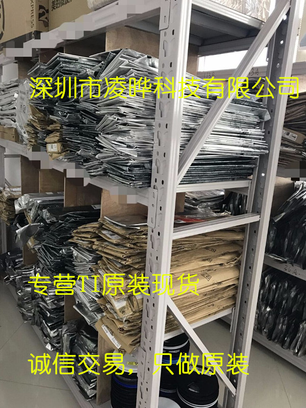
- TPS70448PWP
- 参考价格:
- 发布者:凌晔科技
- 查看更多 TPS70448PWP 供应商 获取更低报价
|
查看此店铺所有供求信息 联系人:陈小姐 电话:13544017528 手机:13544017528 地址:广东省深圳市福田区中航路华强广场C座13L 服务: 价格: 综合: 营业时间:全年营业 QQ/微信/Skype: |
详细信息
品牌:TI德州
封装:HTSSOP-24
批号:18+
数量*:280000
描述:TPS7A89 - 器件与被比较器件具有相似功能,但并不功能等效。 TPS7A89 is the next-generation version of this device.
TPS70448
The TPS704xx family of devices consists of dual-output, low-dropout voltage regulators with integrated SVS (RESET, POR, or power on reset) and power good (PG) functions. These devices are capable of supplying 1 A and 2 A by regulator 1 and regulator 2 respectively. Quiescent current is typically 185 μA at full load. Differentiated features, such as accuracy, fast transient response, SVS supervisory circuit (power on reset), manual reset input, and independent enable functions provide a complete system solution.
The TPS704xx family of voltage regulators offers very low dropout voltage and dual outputs. These devices have extremely low noise output performance without using any added filter bypass capacitors and are designed to have a fast transient response and be stable with 47-μF low ESR capacitors.
These devices have fixed 3.3-V/2.5-V, 3.3-V/1.8-V, 3.3-V/1.5-V, 3.3-V/1.2-V, and adjustable voltage options. Regulator 1 can support up to 1 A, and regulator 2 can support up to 2 A. Separate voltage inputs allow the designer to configure the source power.
Because the PMOS device behaves as a low-value resistor, the dropout voltage is very low (typically 160 mV on regulator 1) and is directly proportional to the output current. Additionally, since the PMOS pass element is a voltage-driven device, the quiescent current is very low and independent of output loading (maximum of 250 μA over the full range of output current and full range of temperature). This LDO family also features a sleep mode; applying a high signal to EN1 or EN2 (enable) shuts down regulator 1 or regulator 2, respectively. When a high signal is applied to both EN1 and EN2, both regulators enter sleep mode, thereby reducing the input current to 2 μA at TJ = +25°C.
For each regulator, there is an internal discharge transistor to discharge the output capacitor when the regulator is turned off (disabled).
The PG1 pin reports the voltage condition at VOUT1. The PG1 pin can be used to implement a SVS (RESET, POR, or power on reset) for the circuitry supplied by regulator 1. The PG2 pin reports the voltage conditions at VOUT2. The PG2 pin can be used to implement a SVS (power on reset) for the circuitry supplied by regulator 2.
The TPS704xx features a RESET (SVS, POR, or power on reset). RESET is an active low, open drain output and requires a pull-up resistor for normal operation. When pulled up, RESET goes into a high impedance state (that is, logic high) after a 120-ms delay when both of the following conditions are met. First, VIN1 must be above the undervoltage condition. Second, the manual reset (MR) pin must be in a high impedance state. To monitor VOUT1, the PG1 output pin can be connected to MR. To monitor VOUT2, the PG2 output pin can be connected to MR. RESET can be used to drive power on reset or a low-battery indicator. If RESET is not used, it can be left floating.
Internal bias voltages are powered by VIN1 and require 2.7 V for full functionality. Each regulator input has an undervoltage lockout circuit that prevents each output from turning on until the respective input reaches 2.5 V.
产品特性
Dual Output Voltages for Split-Supply Applications
Independent Enable Functions (See Part Number TPS703xx
for Sequenced Outputs)
Output Current Range of 1 A on Regulator 1 and 2 A on Regulator 2
Fast Transient Response
Voltage Options: 3.3-V/2.5-V, 3.3-V/1.8-V, 3.3-V/1.5-V,
3.3-V/1.2-V, and Dual Adjustable Outputs
Open Drain Power-On Reset with 120-ms Delay
Open Drain Power Good for Regulator 1 and Regulator 2
Ultralow 185μA (typ) Quiescent Current
2μA Input Current During Standby
Low Noise: 78μVRMS Without Bypass Capacitor
Quick Output Capacitor Discharge Feature
One Manual Reset Input
2% Accuracy Over Load and Temperature
Undervoltage Lockout (UVLO) Feature
24-Pin PowerPAD™ TSSOP Package
Thermal Shutdown Protection
深圳市凌晔科技有限公司
广东省深圳市福田区华强广场C座13L
Tel:13544017528
qq:869030400
E-mail:869030400@qq.com
法律声明:本站只提供信息交流平台,各交易者自己审辨真假,如有损失,本站概不负责。
警方提示:网上买、卖商品要谨慎小心,以免上当受骗。
警方提示:网上买、卖商品要谨慎小心,以免上当受骗。
所有评论
商品评论()
最新评论


